Sleepy Pony @ Cyber Apocalypse 2024 CTF!
Vol 2: The PROM
Preface
This is my first time trying my hands on a CTF event: HackTheBox Cyber Apocalypse 2024! I'm no hacker, but this event has a hardware category, so my friend invited me to a team to try them out. It turned out better than I thought! I was able to solve all of the 5 hardware CTFs! And here's my writeup.
The PROM - Medium
Problem Statement
After entering the door, you navigate through the building, evading guards, and quickly locate the server room in the basement. Despite easy bypassing of security measures and cameras, laser motion sensors pose a challenge. They're controlled by a small 8-bit computer equipped with AT28C16 a well-known EEPROM as its control unit. Can you uncover the EEPROM's secrets?
What's Provided?
- A Docker instance
Capturing the Flag
Important Note: This CTF used to contain bugs on the first couple days of the event. This writeup is made based on the fixed version.
Upon connecting to the terminal, we are welcomed by this lovely help message about a chip AT28C16. (Really, I love that ASCII art! It looks great!)
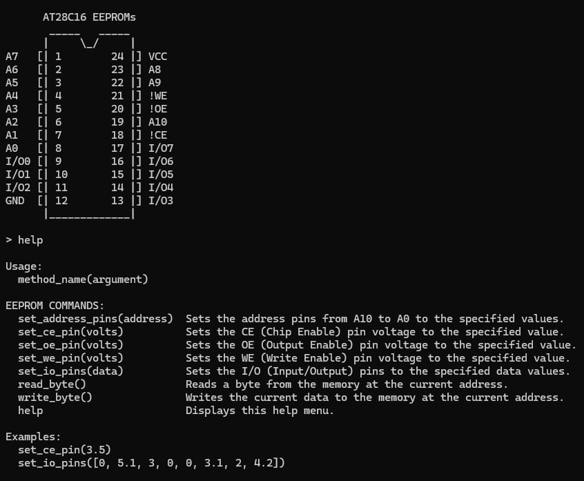
The PROM Help Message
Let's Talk about the PROM
Unfortunately we are not talking about a prom event here. The PROM mentioned in this CTF is an abbreviation for Programmable Read Only Memory. You might not noticed it, but these tiny chips, big and small, are used everywhere a circuit designer need to store something. From storing a configuration data, to your computer's BIOS, to data logging, they are the hidden gem that make our world running.
Specifically for this CTF, we are working with a Microchip (former Atmel) Parallel EEPROM chip AT28C16. You can grab a datasheet from here to follow along.
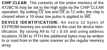
AT28C16 is an EEPROM (Electronically Erasable and Programmable Read Only Memory) unlike ROM and PROM that cannot be erased at all, or EPROM that would need a UV Eraser to erase it, you can read, write, and erase the data on the EEPROM with just electronics circuits. This particular chip can store 16 kilo-bits of data in an 8-bit architecture, i.e. 2048 bytes of data. Communication with this chip is easy but tedious. Parallel protocol means you will need quite a lot of wires to read and write stuff. There are three control pins: (!CE, !OE and !WE), 11 address pins, and 8 I/O data pins you need to control. We will go into details later on the next section.
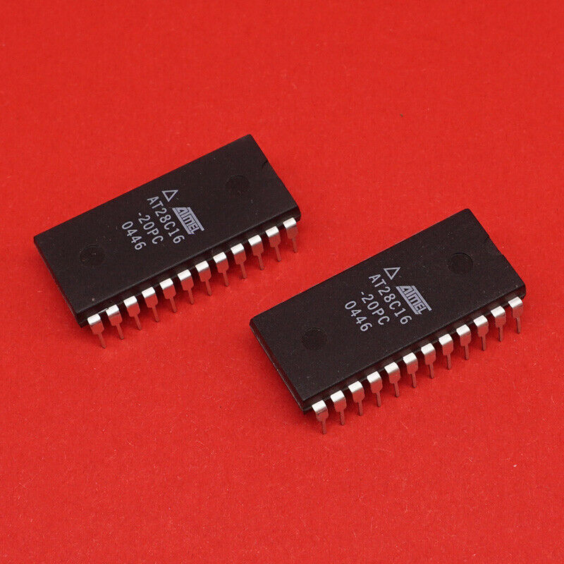
Real Life AT28C16 in a DIP-24 Package (Source: eBay)
Playing with the Chip
From the help menu, there are not that many things we can do with the chip (it is a very rudimentary chip):
- Set the voltage on the !CE, !OE, and !WE pins.
- Set the voltage on each of the 11 address pins.
- Set the voltage on each of the 8 I/O pins.
- Read and write data from/to the I/O pins one byte at a time.
Due to the bug in the simulation, we discovered a lot of details in the CLI while trying to enable the chip:
- The
set_address_pinsandset_io_pinscommands do validate the inputs well so you cannot enter invalid config. - The
set_address_pinsandset_io_pinscommands parameters are MSB-first. - The
read_byteandwrite_bytecommands also do check if the chip is in the correct config before proceeding. - If you use it wrong enough, the chip will release smoke. You have to disconnect from the terminal and reconnect if this happens.
- The !OE pin and A9 pin both support 12V input, just like in the datasheet.
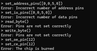
Some Example of CLI Inputs
Reading from the Chip
To read a byte from this chip, you need to do the following:
- Set the !CE (Chip Enable) pin low.
- Set the !OE (Output Enable) pin low.
- Set the !WE (Write Enable) pin high.
- Set the address on the A0-A11 pins to the address you want.
- Probe the data on the I/00-I/07 pins.
- Repeat step 4 and 5 as much as you need.
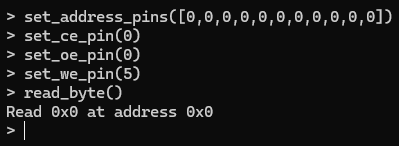
Example Byte Read Step
It's all empty!
After some random read across all address range, we found that every address are 0x00 - it's all empty! (Well, technically empty memory chips are all 0xFF, that's how they physically work, but whatever.)
Going back to the findings above, we know that the !OE pin and A9 pin both support 12V input. Weird right? Why would you need that? The !OE pin uses this voltage as part of a chip-erase operation. (Note that this also works alongside the !WE pin as a write-protection mechanism.) And the A9 pin uses this to read the Device Identification Block. It is another 32 bytes of memory hidden in plain sight!
How long would you take to notice this in the datasheet?
Reading the Secrets Out
Now to dump the Device Identification Block, we have to raise the A9 pin to 12V and read from address 0x7E0 to 0x7FF. Looks like there's something here! You can use a script to do it, or do it manually since it's just 32 bytes.
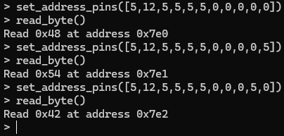
We have something here!
At the end we got these bytes out (in hex)
		    48 54 42 7b 41 54 32 38 43 31 36 5f 45 45 50 52

			4f 4d 5f 73 33 63 32 33 74 5f 31 64 21 21 21 7d
Which could be converted to our flag! Which is...
HTB{AT28C16_EEPROM_s3c23t_1d!!!}
~~~~~